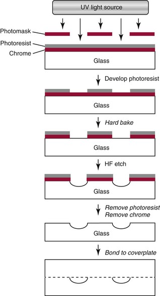
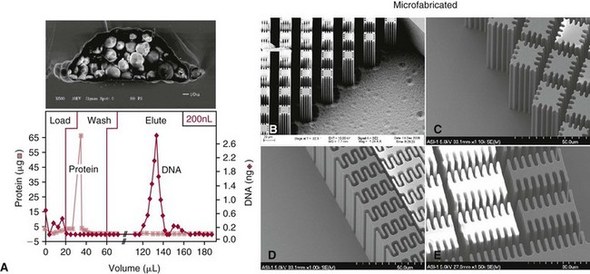
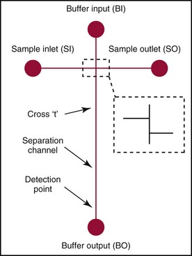
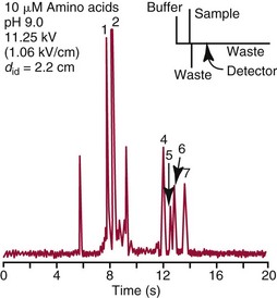
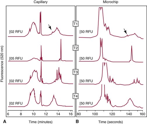
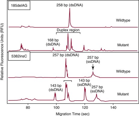
Chapter 18 The first miniaturized analytical device with some degree of functionality was reported in 1979, when the separation of a simple mixture of low molecular weight compounds was achieved in only a few seconds in a microdevice fabricated in silicon.156 The significance of this development can be appreciated only by a relativistic view of state of the art separation techniques common to the laboratories of that time. The 1970s saw most chemical separations carried out using open-column, paper, and thin-layer chromatographic processes, while gas chromatography (GC), having experienced several decades of development, was only beginning to mature into a bona fide technology for small molecule analysis. Pressure liquid chromatography began to evolve into a method that would bring faster analysis times with higher resolution, and the late 1970s saw new chemistries amenable to reverse-phase liquid chromatographic separations for improved resolution of similar compounds. Electrophoresis was the workhorse for large biomolecule separations, with Laemmli having established denaturing separations of proteins in acrylamide gels81 and O’Farrell having just defined the power of two-dimensional (2D) gel separations for proteins119; the advent of sequencing gels137 and the use of agarose gels for nucleic acid separations followed later that decade. On that backdrop, envision the stark contrast of a paper that described a gas chromatographic analyzer fabricated out of silicon (Figure 18-1) using the tools under development for a microelectronics industry that was still in its infancy. The work of Terry and associates156 provided the first evidence that microfabrication could be used to create microminiaturized devices for analytical separations. Despite that, the scientific community did not immediately recognize the significance of this achievement nor see this as a glimpse into a future that would be seeded, in no uncertain terms, by Widmer’s group at CIBA in Basel, Switzerland, roughly a decade later. Although several papers followed this initial work, it was not until the concept of a total analysis system (TAS), first proposed by Manz and colleagues in 1990,104 that the idea of miniaturization had a significant impact. The TAS concept was originally motivated by a lack of adequate sensors for detection of specific species from a complex mixture. It was hypothesized in the seminal Manz paper104 that, by improving the sample treatment steps and thereby increasing the selectivity of the sensor, an ultrasensitive sensor would not be required if interfering chemical compounds were removed. A TAS, as proposed, entailed initial sampling, transport of the sample, sample pretreatment steps, and final detection of the analyte. Miniaturization of all of the processes required for total analysis, a micro–total analysis system (µTAS), would allow development of a TAS that performs these functions at the site of measurement. Additional benefits are derived from decreasing the size of a TAS, such as decreased volumes of sample and reagent and the potential for drastically reduced analysis times. In standard photolithography practices, glass is obtained with a photoresist and metal layer deposited onto the wafer (see Figure 18-2 for a schematic of the process). The function of these films is twofold: to allow for channel design and for glass protection during the chemical etching step. A chrome metal layer is first deposited onto the glass because of its tight bonding with both glass and silicon. This layer provides extra protection from hydrofluoric acid (HF) during wet chemical etching. On top of the metal is a layer of photoresist that allows for channel patterning. The traditional mode of application is to spin-coat the photoresist on top of the metal layer, although there are alternatives to this approach, such as the constant-volume injection method.92 Because such fine precision can be attained using photolithography, application of the photoresist is performed under cleanroom conditions using specialized instrumentation. In most cases, glass can be purchased with both the photoresist and metals already applied. Glass channels are achieved by wet chemical etching using a solution of HF. The etching rate of the solution depends on the concentration of HF in the etching solution—the higher the concentration of HF, the faster the etch rate. An etch rate of 10 µm/min can be achieved with a 49% HF etch solution87 in borosilicate glass. The use of wet chemical etching results in an isotropically etched channel, where the glass is etched equally in all directions. This type of etching results in a channel architecture that has a semihemisphere shape (see Figure 18-2). Once the channels have been etched to their desired width/depth, access holes are drilled and the devices bonded. For glass-glass bonding, thermal bonding is widely used. With this technique, both glass wafers to be bonded are thoroughly cleaned, aligned, and brought into intimate contact. The bonding process takes place at a temperature of 620 to 690 °C over 6 to 8 hours and can be achieved using a programmable furnace. Multiple bonding cycles are typically required to get a fully bonded device, which is one of the biggest drawbacks to thermal bonding. Other approaches have been developed, such as room temperature bonding techniques,17,57,67,128 UV-curable adhesives,59,141 and silicate solutions.63,78,139 Application of a photoresist requires a spin-coater and cleanroom conditions, which can be fairly expensive. Alternatives to the use of a photoresist have been developed, where patterned polydimethylsiloxane (PDMS) was affixed to the glass wafer to be etched and HF flowed through the PDMS channels.134 Enzyme nanolithography has achieved nanometer-sized depressions in a protein surface. Scanning probe microscopy was used to control a nanopipet, which delivered proteases to a dried bovine serum albumin film.61,62 Although wet chemical etching does not require expensive instrumentation, the desire for high aspect ratio structures or for more control over the dimensions of the channel can lead to other types of etching techniques. For example, high aspect ratio structures were obtained in glass and fused silica wafers by using powder blasting,7 fast atom beam etching54 and deep reactive ion etching (DRIE).16 All of these methods involve bombarding the wafer surface with particles; however, DRIE uses chemically reactive ions, typically fluoride, to collide and remove surface atoms while fast atom beam etching uses neutral particles. Because of the expense involved in the fabrication of glass microchips, interest is increasing in the idea of using plastic materials as microfluidic substrates. Some of the key factors to consider when choosing a polymeric material for microchips include surface chemistry, optical clarity, chemical compatibility, temperature stability, and desired application. Glass microfluidic devices make an excellent platform for electrophoretic separations that utilize electro-osmotic flow (EOF), because of the abundance of silanol groups on the surface. This same surface can be difficult in applications such as polymerase chain reaction (PCR), because the glass surface can react with necessary components, thereby inhibiting the reaction. Polyimide is a thermoplastic polymer with a neutral surface charge that provides an excellent vessel for PCR,37 yet it has less than optimal visible light transmittance, making optical detection difficult with this material. Another driving force for finding alternatives to glass for microfluidics involves generally easier fabrication methods. As the list of possible substrates for microfluidic devices grows, ways of making fabrication easier and more streamlined with these materials are becoming more innovative. Polyester-toner microdevices have been made on overhead transparencies using laser printers.20,21,26 The channel geometry is simply printed onto the transparency (where the absence of toner dictates the channels) and placed together with another piece of blank transparency containing only access holes. The sandwich is bonded by lamination, and the toner printing results in channels that are approximately 6 µm deep. These microchips have been used for electrophoretic separations using a number of different detection methods. SU-8 is a negative photoresist that has been used as a substrate for microfluidic devices. Fabrication of these devices takes advantage of the photoresist properties of SU-8 and allows the device to build in a number of layers.162 The first layer is homogeneously spun onto silicon; this is followed by complete cross-linking with UV exposure. A second layer is spun onto the first layer and covered with a photomask during UV exposure, which allows the channel pattern transfer. The third layer is separately spun onto a piece of glass, completely cross-linked through UV exposure, and then placed onto the second layer. A low-temperature baking step, UV exposure of the whole device, and removal of the glass and silicon pieces complete the device. Thermoset polyester (TPE) is an unsaturated polyester in which cross-linking occurs upon addition of a catalyst; TPE can be fabricated using many of the same techniques as are used with PDMS (see section later).166 Poly(cyclolefin), the same material used in making compact discs, has also been used in microfluidic devices.73 Hot embossing is used to make these chips, and a silicon master allows for channel dictation. A cover plate is bonded to enclose the device, using heat and pressure to generate a complete seal. Polydimethylsiloxane (PDMS) is one of the most popular polymeric materials used as substrates. Fabrication is fairly easy involving the combination of elastomeric base and curing agent. The PDMS surface has methyl groups on the surface, imparting a hydrophobic nature, and is flexible and optically transparent. The flexibility of PDMS allows it to be a highly chosen substrate for valving, and it can be both reversibly and irreversibly5,6,73 sealed to a variety of surfaces. Several different PDMS fabrication methods have been reported (see Sun151 for a review), with replica molding73 and rapid prototyping being two processes that are readily used. Rapid prototyping involves the use of a master, which, once made, allows for fast and easy replication of that design. The master is made by using a negative photoresist, such as SU-8, spun onto a silicon or glass wafer. The microfluidic channel design is imparted onto the photoresist using photolithography and the wafer subsequently developed. Because SU-8 is a negative photoresist, only where the light is incident is where the photoresist is rendered insoluble, while the remaining photoresist remains soluble in the developer solution. This leaves photoresist only where the channels are, exposing the glass everywhere else. Etching of the glass results in the reverse architecture of the glass microfluidic layer, where the channels are raised instead of imprinted. The height of the photoresist over the glass dictates the depth of the PDMS channels. Although photolithography is still used in fabrication of the master, once made, multiple devices can be made easily. PDMS is produced when an elastomeric base and a curing agent are mixed in the appropriate ratios. Once mixed, they are poured over the master and are allowed to cure; this can happen at room temperature overnight, although heating quickens the process. The cured PDMS can then be peeled from the master and bonded with the substrate of choice. The bonding method will depend on the substrate used for the coverplate; PDMS/PDMS devices can be reversibly bonded by putting the two pieces into contact with one another. Irreversible bonding of PDMS/PDMS can be achieved through a number of different methods, one being activation of the surface by plasma oxidation.6,73 Liu and coworkers reported another method, in which they altered the elastomer base to curing agent ratios, using 20 : 1 for the fluidic layer and 5 : 1 for the cover plate. The device was assembled and placed in an oven, at which point the two layers fused as the result of the distribution of excess reagents between the two layers.5 Poly(methylmethacrylate) (PMMA) has become a popular substrate choice for microfluidic devices. PMMA is considered a thermoset polymer that softens into a viscous liquid when heated above its glass transition temperature. Multiple methods of fabrication are available, and the channel surface is easily modified to adapt to a particular application; see references 6 and 151 for reviews of polymer fabrication techniques. Hot embossing80,131 is a technique that can be used with a variety of substrates; it consists of heating the polymer above the glass transition temperature and stamping the substrate with the desired microfluidic pattern. To make PMMA devices using this technique, a metal or silicon stamp is brought into contact with the PMMA and is embossed using a constant force and elevated temperatures to partially melt the substrate. The embossing process can be completed in less than 10 minutes, and once the apparatus has cooled, the stamp and the substrate can be carefully separated. This same process can also be done at room temperature using PMMA as a substrate; this yields channel dimensions that vary by less than 2%.184 Injection molding, another fabrication technique used to make PMMA devices,29 incorporates the use of a metal or silicon stamp. This involves heating the PMMA at high temperatures, which results in the formation of a viscous liquid. The PMMA is then pushed into the mold by applying high pressure and is allowed to cool; it is then removed from the mold. Both of these methods result in devices with micron-sized channels and are useful for mass production of devices with the same microfluidic pattern. Certain applications require the use of sub–micron-sized features; x-ray lithography is capable of making these small channels and intricate structures. Figure 18-3 shows an example of post structures that can function as a solid phase for DNA chromatography. Solid phases for DNA extraction traditionally are created with silica beads, sol-gels, or silica bead/sol-gel hybrids (see section on DNA extraction). However, phases can also be microfabricated during the microchip fabrication process. This can be done by using a direct write process or a mask, typically fabricated in a thick gold layer because it can absorb the x-rays. Where the x-rays are incident upon the PMMA, the polymer degrades. The device is placed into a developer solution which removes degradation products by solubilization. The length of exposure along with the energy used dictates the depth of the channels. Laser ablation is also used to make submicron features in PMMA devices. This involves bombarding the surface with a pulsed UV source to damage the polymer structure.149 With both of these last two techniques, high aspect ratio features can be accomplished; however, neither of these methods is ideal for situations involving mass production of the same design. Miniaturized electrophoresis was the first and most dominant embodiment of a µTAS, with the driving force for the miniaturization related to an enhancement in its analytical performance, rather than a simple reduction in size.104 Because separation efficiency is a function of the applied voltage, microfluidic devices use shorter separation lengths, along with application of high voltages typical of capillary separation, resulting in fast, efficient separations. A core component in the development of microfluidic technology has been the use of microchips as an analytical platform for electrophoretic separation.46 Components required for microchip-based electrophoresis (ME) include a detection system, a power supply, and a computer with programmable software for controlling application of voltage, for data collection, and for conditioning of raw data. A number of different detection systems can be used with microchips; however, a fluorescence detection system, essentially a home-made fluorescence microscope, is the most widely used.46 In terms of selection of the components, power supply selection is critical, because a required number of voltage outputs are needed for electrokinetic injection of the sample and application of the desired electric field. For chip-based separations, the cross-t design originally proposed by Verheggen and associates165 for electrokinetic injection of sample is the most popular. With this design, a minimum of four voltage outputs are required to control the sample injection and separation. As the complexity of the chip design increases, more outputs may be necessary, particularly if electrokinetic pumping of reagents and buffers is involved. The user is cautioned, however, that effective electrokinetic mobilization of solutions through the microchip architecture is limited to reagents that are low in conductivity and not high in organic solvent concentration; this results in obvious limitations with many clinical samples and, thus, may necessitate the implementation of pressure-driven fluidic control. For injection, both pressure-driven and electric field–driven injection modes are used, as they are in capillary electrophoresis (CE). The pressure-driven injection mode commonly used in CE, which avoids bias associated with analytes that have a wide range of electrophoretic mobilities, is less popular with chip-based injection. That said, Karlinsey and colleagues77 demonstrated that integrated diaphragm pumps on a hybrid PDMS-glass microchip could perform pressure sample injection for subsequent electrophoretic separations. The same type of electrokinetic bias associated with CE could be avoided on-chip with pressure injection, and pressure injection could be achieved with sample volumes as low as 500 nL while sample composition was maintained. This was later used by Easley and colleagues32 for integrated microchip detection of infectious pathogens in blood. However, the injection mode that dominates for most applications in microchip electrophoresis is electrokinetic injection (driven by electrophoretic mobility and/or electro-osmotic effects). The more popular electrokinetic sample injection is dominated by two types—pinched and gated—that are used in standard cross-t design chips. With the pinched injection, a small sample plug is electrokinetically mobilized into the injection cross-t via a voltage applied between the sample and the sample waste reservoir and orthogonal to the separation channel.65 Once the cross-t is adequately populated with sample, sample injection is accomplished by reconfiguring the primary electric field between the inlet buffer and the outlet buffer reservoirs. Injection “bleed” of sample into the separation channel is minimized by applying a small voltage to the sample and the sample waste. A gated injection allows the sample to electrokinetically migrate through the cross-t toward the sample waste reservoir and then is directed into the separation column by temporarily terminating the potential at the buffer reservoir via a high-voltage relay and allowing the sample to migrate into the separation channel electrokinetically.66 Unlike a pinched injection, the injected plug volume is dependent on the amount of time the buffer reservoir potential is off. Additionally, this type of injection is susceptible to bias based on differences in analyte electrophoretic mobility. When chip-based separations are performed, the separation channel in a cross-t design provides the counterpart of the capillary in CE, although with a substantially truncated separation length (Figure 18-4). Many of the parameters governing electrophoretic separation in capillaries apply to chip-based separations. For example, like capillaries, one of the benefits of glass-based devices is their inherent ability to dissipate the Joule heat generated from use of the high electric fields needed to facilitate rapid separation. However, the same type of Ohm’s law plot (applied voltage vs. current) that would be used to test buffer compatibility with high electric field application should be carried out here as well.83 Using the appropriate buffer for the separation of interest, the channel surface must be conditioned in a manner not dissimilar to those processes used with capillary systems. If separations requiring EOF are performed, the rigorous cleaning method suggested for fused silica capillaries is required to ensure proper surface regeneration, but attention must be paid to hydration of the glass. The entire cross-t channel architecture of the device is filled, including the reservoirs, to ensure good electrical contact between the platinum electrodes and the solution. The holes drilled into the microfluidic device to function as reservoirs (i.e., buffer/sample microvials) may not be large enough to hold a sufficient volume of buffer to avoid buffer depletion. The user must remain cognizant of this and, even with expanded reservoirs generated by commercial “nanoports,” or homemade trimmed pipette tips, replenishment of the buffer may be needed. For sample injection, separation, and detection in a chip of simple design (see Figure 18-4), the sample is placed in the reservoir (SI) and a voltage is applied between SI to SO to inject the sample into the separation channel in a manner consistent with the injection mode chosen. Separation is initiated by application of voltage to BO and BI where electrophoresis of the sample analytes down the separation channel ensues. A point along the separation channel, most commonly at a location close to BO, is used for detection. The detection mode most commonly used is optical detection, and laser-induced fluorescence is popular because of its sensitivity. The detector system [e.g., a laser and photomultiplier tube (PMT)] is positioned at a point in the separation channel commensurate with providing the necessary effective separation length (Leff) for the separation; sample analytes passing that detection point are excited, and the resultant fluorescence is collected. Although the electric fields (E; volts/cm) applied in microchip electrophoresis approach (but do not exceed) those used in capillaries, reduction of the Leff is more easily achieved in microchips. The reservoirs and electrodes required to apply voltage to capillaries limit the minimal Leff to tens of centimeters; microchips, in contrast, can easily allow for separation distances of a few centimeters. It is interesting to note that the U-shaped channel in microchips has little effect on the resolution of separations under high electric fields. The plug profile typically associated with capillaries and known to play a role in yielding high-efficiency (number of theoretical plates) separations does not seem to be adversely affected by the semihemispherically shaped channels. A detection system is required to measure the number and quantity of analytes electrophoretically separated in the channel as they pass the detection point. With increasing popularity of microchips for separation, a variety of different detection options have evolved that include optical detection methods that are, for the most part, similar to those employed in CE. However, electrochemical, conductivity, and mass spectrometric approaches have also been developed. For optical detection, the most prevalent method in CE and high-performance liquid chromatography (HPLC)—ultraviolet-visible spectroscopy (UV-VIS) detection—is not as common with chip-based electrophoresis, primarily because of challenges with the short optical path length (channel depth) in miniaturized systems and the difficulties involved in coupling light into and out of these channels.167 That said, a number of reports have detailed progress with UV-VIS detection in analytical microsystems.10,28,41,91,102,108,183 However, no universally successful method akin to that on CE has been devised. A number of other optical detection schemes for microchips have evolved with varied success and applicability, including infrared,126 nuclear magnetic resonance (NMR),175 surface plasmon resonance,74 thermal lens microscopy,161 and chemiluminescence/electrochemiluminescence.55 The most prevalent detection system used for chip-based separation is laser-induced fluorescence (LIF).71 It not only is an extremely sensitive method for detection in chemical separations (subzeptomole detection limits), it also is well suited to detection in small volumes, hence, its widespread popularity in capillary electrophoresis separations. A number of reviews have detailed the components required for LIF, have provided a guide to alignment of the optical system, and have described the keystone elements (analyte velocity, probe volume, optimized signal-to-noise ratio as a function of excitation intensity) necessary to achieve sensitive detection.71,75 Components of an LIF system consist of a light detection module, such as a photomultiplier tube or a charge-coupled detector (CCD) camera, a laser source, optics for alignment of the excitation/emission, an excitation source, and a computer for data collection. LabVIEW software (National Instruments, Austin, Tex), which is commonly used as the interface, allows easy application–specific computer programming to provide software interfaces that permit collection of data and control the detection system.71,75 A typical method for performing LIF detection on a microchip is to bring the excitation light from a laser of light-emitting diode into the microchannel orthogonal to the device plane, which is relatively simple to align, and to then focus the beam into the channel using a microscope objective or some combination of achromatic lenses. LIF emission is collected with a separate objective or lens combination, spatially and spectrally filtered, and recorded on a photodetector. Confocal detection systems were popular in the capillary electrophoresis literature early on,51 when focusing and collection optics were one and the same, and the excitation and emission wavelengths were separated with a dichroic beam splitter. Variations in LIF detection setup exist, however, and He and colleagues presented a detailed illustration of their laser-induced detection system, in which excitation is brought into the microchannel from an angle.50 Two relatively recent reviews provide detailed descriptions of the fundamentals and practice of LIF detection in microanalytical systems.71,75 Chip-based detection systems can involve multipoint detection in a single channel or the multichannel detection that is key to high-throughput analysis. For multipoint detection, waveguides can be incorporated into the microchip design for detection at multiple points along the same channel109 and applied to microchip isoelectric focusing (IEF).42 Yao and coworkers186 carried out whole channel imaging during the IEF separation of proteins using a CCD array, ironically using organic LEDs as the excitation source. Alternatively, Raisi and coworkers used a scanning fluorescence detector and a single PMT to scan the entire separation channel.132 In terms of multichannel scanning, Huang and associates used an acousto-optic deflector (AOD) to change the diffraction angle of an incident laser beam to address an eight-channel device designed for parallel DNA separations.58 However, the most significant advances have involved the multichannel microdevices designed by Mathies and coworkers for high-throughput analysis. Paegal and colleagues multiplexed 96 channels on a radial capillary electrophoresis microchannel plate,125 demonstrating that the microchip platform could compete with the 96 capillary arrays that had evolved for CE. Radial microdevices of this ilk for DNA analysis containing as many as 384 channels34 have been demonstrated as possible.143 More recently, this group reviewed the types of applications possible with these high-throughput chip-based systems.95 Multicolor LIF detection is not essential for all applications but certainly for some involving key genetic analysis techniques. Expanding the number of photodetectors needed to sample at multiple emission wavelengths is the simple approach that has been used for multicolor DNA sequencing98 and genotyping142 on microchips; however, Backhouse and associates used a diffraction grating to disperse the LIF emission onto a CCD array for four-color sequencing,2 and Simpson and colleagues used a transmission imaging spectrograph with a wide imaging area to disperse LIF emission from a two-color genotyping experiment run in 48 parallel channels onto a CCD array.144 More recently, a system was developed to complement the microchip platform by featuring a single acousto-optic tunable filter (AOTF) and a single PMT.76 The filter behaves similarly to the previously described AOD, except that when an acoustic wave traveling through the crystal at a specific frequency interacts with the light, only select wavelength bands are diffracted by the crystal and collected by the PMT.75 Although small molecules were the target analytes in early chip-based separations (fluorescein and calcein),47,105 the separation of amino acids46 (Figure 18-5) changed the landscape to one that could involve biomolecules of interest and eventually led to a literature dominated by the separation of DNA fragments using laser-induced fluorescence as the detection method. The significance of the early studies showing electrophoretic separation of analytes in a planar glass system was less about faster analysis times and more about the drastic reduction in reagent consumption. It was this unprecedented analytical potential that paved the way for DNA separations in microdevices, shoring up the threat that CE was bringing to large, unwieldy slab gels that were slow to run, cumbersome to manipulate, and labor intensive to use in high-throughput mode. Early work from Mathies and coworkers laid the groundwork for successful separation in 120 seconds of ΦX174 Hae III restriction fragments ranging from 70 to 1000 bp.180 This technology was advanced by this group, which accomplished high-resolution separations and DNA sequencing using multicolor fluorescence detection.97,179 Although Karlinsey and associates showed that using an AOTF for multicolor detection could be applied to short tandem repeat (STR) profiling for human identification, the microchip-based separation of amplified gene products for STRs of clinical significance has also been demonstrated. For example, fragile X syndrome has been correlated with a CGG repeat expansion seen in the 5′-untranslated region of the familial MR type I (FMR1) gene. Individuals with the premutation show an unstable number of (CGG)n repeats and generally are asymptomatic; however, identifying the number of trinucleotide repeats is critical for genetic counseling. Sung and colleagues152 used microchip separations that were completed in less than 1 minute to identify these trinucleotide repeats using a polymethyl(methacrylate) (Plexiglas) microchip; this represented a roughly 100-fold reduction in analysis time when compared with the 70 minutes consumed by the conventional slab gel approach. Similarly, Cantafora and colleagues14 used microchip electrophoresis to detect the D19S394 tetranucleotide repeat (AAAG)n. This repeat is highly polymorphic (with the number of repeats typically ranging from 1 to 17) and is a short recombination distance from the low-density lipoprotein (LDL) receptor gene, making it suitable for the study of familial hypercholesterolemia (FH). Analysis was performed using the commercial microchip electrophoresis system, with instrument control by dedicated software for completely automated sample injection, fluid manipulation, and data collection. This system is designed to analyze 25 to 500 base pair (bp) double-stranded (ds)DNA fragments with 5 bp resolution. Using this, 70 carriers of two LDL receptor mutations common in Northern Italy were compared with 100 healthy controls, and the microchip-based technique was successfully used for the sizing of D19S394 needed for a simple cosegregation analysis. Nemoda and coworkers117 used a microchip with 96 robotically loaded electrophoretic lanes for analysis of 20 bp repetitive sequence elements within the 5′-regulatory region of the serotonin transporter gene (5-HTT). Two amplified products, one for each of two common alleles (a short 14-repeat and a long 16-repeat sequence), that were shown to have an impact on transcription of this key synaptic transporter, could be separated and detected in about 4 minutes. The reduction in analysis time for the 334 samples that were genotyped for variable repeats was dramatic in comparison with that required for conventional slab gel electrophoresis. This technology was applied in a similar way to the detection of variable repeat alleles of the dopamine receptor (DR) gene using PCR and microchip electrophoresis.4 Following PCR amplification of a variable number of repeats of a 48 bp sequence, chip electrophoresis allowed separation and detection of the products in 90 seconds, highlighting the potential of pharmacogenetic analysis for mutations shown to correlate with effective doses of methylphenidate in school children.43 An early diagnostic application of electrophoretic microchips involved the detection of T-cell receptor (TCR) gene rearrangement, where normal samples yield amplified PCR fragments representative of a polyclonal lymphocyte population, while lymphoma patients display a monoclonal population. Munro and coworkers113 were able to separate B- and T-cell gene rearrangement PCR products on microchips, providing diagnostic information in an assay where the electrophoresis consumed only 160 seconds (Figure 18-6). This marked a 60-fold decrease in analysis time compared with conventional slab gel methods, with no loss in diagnostic capacity. More recently, Legendre and associates85 demonstrated a microchip separation method for analyzing post-PCR products from patients’ samples that were both positive and negative for T-cell lymphoma. They showed the resultant electropherograms, where negative samples show three broad peaks, characteristic of a range of different sized PCR products generated, and positive samples show the presence of one or two strong peaks, caused by the presence of a clonal cell population. These separations required less than 5 minutes on a microdevice—a more than 8-fold reduction in time when compared with commercial capillary electrophoresis. With heteroduplex analysis (HDA), a common method for mutation detection, denaturation of the sample DNA followed by controlled re-annealing generates homoduplexes or heteroduplexes, depending on whether wild-type or mutant DNA is present. The relative presence of these can be parsed out via differences in the electrophoretic mobilities of the duplexes stemming from the degree of sequence mismatch. Tian and colleagues158 used HDA-based electrophoresis to target BRCA1 and BRCA2 germline mutations. Using microchip HDA analysis, they demonstrated the detection of six different deletion, insertion, and point BRCA mutations in separations that were complete in 130 seconds, proving the microchip platform to be a powerful and efficient mutation screening. Similarly, Footz and coworkers36 compared a microchip-based HDA technique versus denaturing HPLC (dHPLC) using glass microchips and a commercial self-coating sieving polymer. They showed that eight sequence variants of BRCA1 and BRCA2 genes could be detected, even without optimization of PCR amplification or of chip HDA conditions, demonstrating that the microfluidic technique could provide sensitivity similar to that of an extensively optimized dHPLC system. An alternative mode of mutation detection, allele-specific PCR (AS-PCR), is commonly used for the rapid detection of known single-base DNA polymorphisms. AS-PCR was used by Medintz and associates107 on a capillary array electrophoretic microplate for high-speed single-nucleotide polymorphism (SNP) analysis of the HFE gene, which is associated with hereditary hemochromatosis (HH). The HH disorder is an autosomal recessive disease of iron metabolism, affecting roughly 1 of every 300 people of Native American descent. The disease has been linked to an S65D (193A>T) substitution. In this analysis, two different fluorescently labeled primers were designed to detect the HH-associated substitution mutation [S65C (193 A>T)], with the A- and T-specific amplicons identified by both size and color. Using microchip electrophoresis on a radial 96-channel array, analysis of 96 samples could be completed in an unprecedented 10 minutes. This work was later extended by Emrich and colleagues34 into a 384-lane microfabricated capillary array electrophoresis device for massively parallel genetic analysis, demonstrating the high-throughput SNP genotyping made possible by microchip-based microchannel arrays. The AS-PCR was also exploited by Tian and coworkers,157 in conjunction with HDA analysis of BRCA mutations. The wild-type homozygotes and heterozygotes were distinguished on the basis of the number of peaks observed after chip-based electrophoretic separation (Figure 18-7). Alleles were identified in less than 180 seconds by microchip electrophoresis, for a total analysis time (including a 10-minute DNA purification and a 1.2- to 2-hour PCR amplification) of less than 2.5 hours. The method was simple and rapid, and because no enzymatic digestion was used, post-PCR processing was not required. Chowdhury and associates18 used microchip analysis to probe gene variants within the thiopurine-S-methyltransferase (TPMT) gene using AS-PCR and restriction fragment length polymorphism (RFLP)-PCR followed by chip-based electrophoresis with multicolor LIF. With both AS-PCR and microchip electrophoresis integrated into a single microchip that accepted off-chip purified DNA, this chip enabled PCR-RFLP-µCE analysis to be performed in 3 hours, compared with 9 hours for conventional methods,18 and over 24 hours with an oligonucleotide array microdevice.116 Excluding prepurification, the costs of the polymeric microchip and reagents used by these authors for a single analysis totaled only $10, demonstrating the potential of microfluidics to provide disposable chips for both reduced sample handling and contamination risk, as well as cost-effective decentralized point-of-care testing. Single-stranded conformational polymorphism (SSCP), developed by Orita and colleagues124 in the late 1980s, involves thermal denaturation of the sample post PCR amplification, followed by rapid cooling (“snap-cooling”), allowing single-stranded oligonucleotides to take on a self-annealed three-dimensional (3D) conformation. The discriminating aspect of this mutation detection method is the fact that the 3D conformation depends on the intrastrand base pair sequence, with different alleles forming differing conformations that can be resolved electrophoretically. For smaller PCR products (<200 bp), SSCP can resolve single base pair mutations with greater than 90% accuracy—this can approach 100% accuracy when coupled with heteroduplex analysis.1,36 Following on their work with HDA, Tian and coworkers160 were the first to implement SSCP on an electrophoretic microchip to detect mutations in two breast cancer genes, BRCA1 and BRCA2. Following multiplex PCR amplification using fluorescently labeled primers and snap-cooling on ice to induce intrastrand secondary structures and separation of the products by microchip electrophoresis, resolution of the fluorescently tagged amplicons was possible in 130 seconds or less, representing analysis speed that was orders of magnitude faster than with slab gel analysis and even capillary electrophoresis. Vahedi and associates164 followed this work with fusion of HA and SSCP on a single electrophoretic microchip. Using the manual addition of formamide to the PCR amplicons from BRCA1 exon 20, and HFE exon 2, they were able to electrokinetically inject into a traditional cross-t microchip, with subsequent separation yielding heteroduplex data. Although the ability to do sequential HA and SSCP on the same microchip with the same sample is advantageous, it is important to recognize that the manual addition of formamide to the sample reservoir removes the ability to repeat the HA analysis. An additional discriminator involves real-time labeling of the heteroduplex and SSCP products with intercalating dyes (as opposed to using fluorescently labeled primers). Shortly after, the same group103 demonstrated that detection of all three major HFE mutations could be accomplished using similar HA/SSCP technology, but again, using the cumbersome manual addition of formamide. Barron’s group addressed the issue of optimization of HA and SSCP on a microchip using PCR amplicons of p53 exons 5 through 9.53 PCR-amplified products were subjected to HA and SSCP via heat denaturation followed by snap-cooling on ice. By evaluating a variety of sieving mediums and channel coatings synthesized and characterized by this group, and by using a high-pressure loading device to accommodate loading of the highly viscous polymers into microchip channels, they identified a polymer (600 kDa linear polyacrylamide) and a hydrophobic wall coating (poly-N-hydroxyethylacrylamide) that seemed to provide optimal resolution of DNA conformational variants by microchip electrophoresis.
Microfabrication and Microfluidics and Their Application to Clinical Diagnostics
Background
Microdevice Fabrication
Photolithography and Glass Etching Techniques
Alternatives to Traditional Photolithography and Wet Chemical Etching
Polymeric Materials
Polydimethylsiloxane (PDMS)
Plexiglas (PMMA)
Separation and Detection of Clinically Relevant Analytes
Electrophoretic Separations
Detection on Microchips
Exemplary Separations
Mutation Detection via Microchip Analysis
![]()
Stay updated, free articles. Join our Telegram channel

Full access? Get Clinical Tree


Microfabrication and Microfluidics and Their Application to Clinical Diagnostics